
In the back-end process stage, wafers (silicon wafers with circuits on the front) need to be thinned on the back before subsequent dicing, bonding and packaging to reduce the package mounting height, reduce the chip package volume, improve the chip's thermal diffusion efficiency, electrical performance, mechanical properties and reduce the amount of dicing. Back grinding has the advantages of high efficiency and low cost. It has replaced traditional wet etching and ion etching processes to become the most important back thinning technology.
Diamond back grinding wheels are used for silicon wafer grinding. our advanced technology makes back grinding wheel possible to grind all types of semiconductor wafers with less subsurface damage.
Wafer thinning is carried out for the purpose of improving thermal performance, adapting to packaging requirements, increasing flexibility, improving device performance and yield. Each step requires precise control and testing to ensure that the thinned wafer can meet the needs of subsequent processes and final products. The thinned chip is smaller in size and can adapt to thinner packaging designs. Smaller size can reduce the overall thickness and weight in devices such as smartphones, tablets, and smart watches. In 3D IC packaging, more layers of thinned chips can be stacked vertically in a limited space to achieve higher functional density.
The thinned wafer has a shorter heat diffusion path and a higher surface area to volume ratio, which helps to transfer the heat generated by the chip faster and more effectively. If the chip is too thick, the heat will accumulate inside the chip during the transfer process, causing local overheating and affecting device performance.
The limit thickness of wafer thinning is closely related to the material and size of the wafer. Larger wafers are more likely to break during the thinning process. The larger the size, the more difficult it is to thin.
Wafers are made of a variety of materials, generally Si, GaAs, GaN, InP, LN, LT, glass, sapphire, ceramics, etc. LN, LT, GaAs, GaN, etc. are more brittle than silicon, so the limit thickness of thinning is larger. Taking silicon as an example, a 12-inch silicon wafer can be thinned to about 50um.
Wafer thinning is a key step in the semiconductor manufacturing process. Its main purposes include the following aspects:
1. Improve heat dissipation performance
Explanation: Wafer thinning can significantly improve the heat dissipation performance of the chip. Thinner wafers can conduct heat away faster, preventing the chip from overheating and improving device reliability and performance.
Steps: The thinned wafer requires thermal management design during the packaging and testing stages to ensure that it can effectively dissipate heat in actual applications.
2. Adapt to packaging requirements
Explanation: Modern semiconductor devices are increasingly pursuing thin, light and short packaging forms. Thinner wafers allow for more compact packaging to meet the small size and light weight requirements of mobile devices.
Steps: After thinning the wafer, subsequent packaging processes, such as flip-chip packaging, are required to ensure the mechanical strength and electrical connection of the thin wafer.
3. Increase mechanical flexibility
Explanation: The thinned wafer is more flexible and can adapt to some specific application requirements, such as wearable devices or flexible electronics.
Steps: After the wafer is thinned, the mechanical strength and toughness needs to be tested in the subsequent process to ensure that it can withstand various stresses in actual use.
4. Improve device performance
Explanation: By thinning the wafer, parasitic effects can be reduced, especially in high-frequency applications. Thinner wafers can reduce parasitic capacitance on the wafer, thereby improving the electrical performance of the device.
Steps: The thinned wafer needs to pass a series of electrical performance tests to ensure its performance improvement in high-frequency applications.
5. Improve yield
Explanation: The thinning process can remove some defects on the wafer surface and improve the final chip yield. Thinning can remove some of the surface stresses and defects introduced during the manufacturing process.
Introduction to four wafer thinning methods
Mechanical grinding (Grinding)
Grinding completely removes material from the wafer surface through physical friction. Grinding usually uses a grinding wheel containing diamond particles to contact the wafer surface while rotating at high speed, and uses pure water as a coolant and lubricant to achieve the purpose of thinning.
Advantages: Rapid removal of large amounts of material, suitable for initial thinning.
Disadvantages: May cause surface damage and stress, and subsequent processes are usually required to improve surface quality.

Chemical mechanical polishing (CMP)
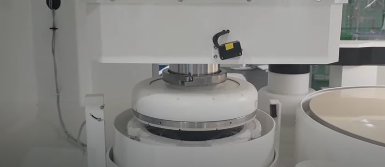
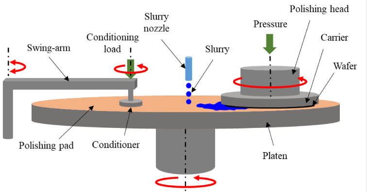
CMP is a technology that combines chemical reaction and mechanical polishing. During the CMP process, the grinding fluid first reacts slightly with the material to be polished to soften the wafer surface, and then mechanical polishing is used to remove the softened material to achieve the purpose of global flattening. Compared with Grinding, CMP is more expensive.
Advantages: It can achieve extremely high surface finish and flatness, suitable for applications requiring high precision.

Wet etching
Use liquid chemicals to remove material from the wafer surface.
Advantages: Low cost, simple equipment, and easy operation.
Disadvantages: Etching is not uniform enough, it is difficult to control the etching depth and profile, and the surface is rough after thinning.
Dry etching
Uses active radicals generated by plasma to remove materials from the wafer surface.
Disadvantages: high cost, complex process, and rough surface after thinning.
In order to avoid indentations during wafer thinning, the following methods can be adopted:
(1) Select matching grinding wheels and abrasives
Select appropriate grinding wheels and abrasives according to the hardness, film thickness and other characteristics of the wafer material. The abrasive size should be gradually reduced to prevent damage caused by excessive abrasives.
(2) Control grinding machine parameters
The grinding parameters, including loading pressure, rotation speed, feed speed, etc., need to be adjusted according to the specific wafer material, size and grinding wheel selected by the grinder.
(3) Maintain the performance of the grinding machine
The grinder needs to maintain normal operating conditions, repair or replace aging parts and grinding wheels, and avoid machine instability or abnormal vibration.
(4) Clean or perform other pre-treatment as needed
Before grinding, the wafer should be properly cleaned or otherwise pre-treated to avoid interference during the grinding process
Wafer thinning generally uses wafer self-rotation grinding, and the processing process includes rough grinding and fine grinding. The axial feed speed of rough grinding is high, and a diamond grinding wheel with a larger grain size is used to quickly remove about 90% of the machining allowance; the axial feed speed of fine grinding is low, and a diamond grinding wheel with a very small grain size is used. The purpose of fine grinding is twofold:
1) Remove the remaining 10% machining allowance;
2) 2) Eliminate the damage layer caused by rough grinding.
Moresuperhard uses a diamond back grinding wheel made of vitrified bond, which is specially used for wafer thinning. vitrified diamond back grinding wheel covers a variety of grain sizes such as 600#, 800#, 1000#, 2000#, 8000#, etc., which can meet the processing needs of different customers. At the same time, the company also has the technical ability to produce 20000#~30000# grinding wheels, and can produce particles ranging from 600#-30000#, which provides the possibility for more sophisticated processing.
In addition, for thinning grinding wheels, Moresuperhard brand back grinding wheel replaces imported Japanese Sumitomo grinding wheels and has been supplying rough and fine grinding thinning grinding wheels to domestic and foreign customers stably:
1. Silicon wafer thinning back grinding wheel
400# 800# 1500# 2000# 6000# 8000# 10000# 15000#
2. Silicon carbide back grinding wheel
400# 800# 1500# 2000# 8000# 15000# 30000# (mostly imported grinding wheels)
3. Plastic back grinding wheel
400# 600# 800# 1000# 1200# 1500# 1800# 2000# 4000#
4. Quartz glass back grinding wheel
600# 800# 2000# 3000# 5000# 8000# 15000#
---EDITOR: Doris Hu
---POST: Doris Hu
Semiconductor Industry Solutions
PCD & PCBN Tools Grinding Industry
Diamond Cutting Bruting Polishing
Add: No.171 Zhongyuan Rd, Zhongyuan District, Zhengzhou, 450001, Henan, China
Tel: +86-371-86545906
Phone / Whats App: +86 18339903057
E-mail: [email protected]


